
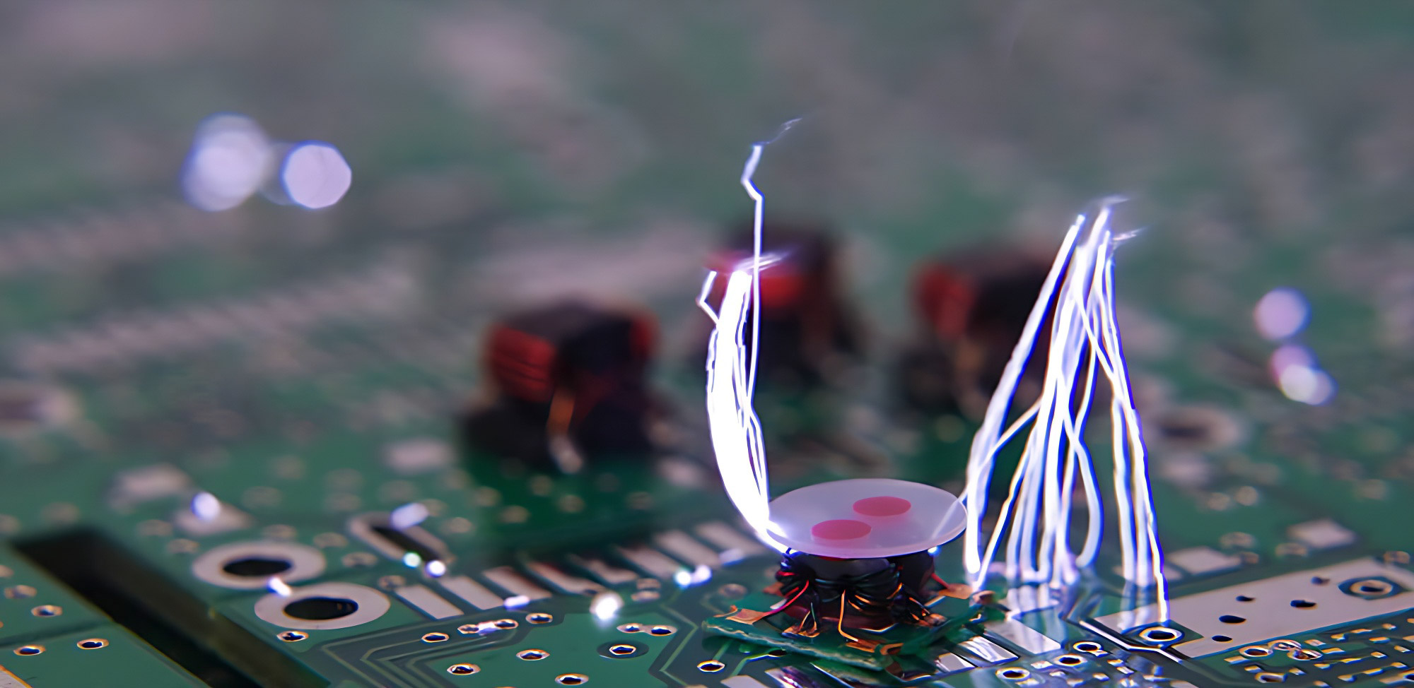
Electrostatic discharge (ESD) protection is critical in PCB (Printed Circuit Board) design, especially for sensitive electronic components and high-precision devices. ESD can damage circuits, degrade performance, and even render products unusable. Below are six professional strategies for designing ESD-resistant PCBs to enhance their reliability and safeguard against electrostatic hazards.
1. Grounding Design
Grounding is a cornerstone of ESD protection in PCB design. An effective grounding strategy ensures that static charges are safely dissipated into the ground, protecting electronic components on the board.
- Multi-point Grounding: Incorporate multiple grounding points across the PCB to allow static charges to disperse rapidly. This is commonly used in multilayer boards, reducing resistance and inductance.
- Large Ground Plane: Utilize extensive ground plane areas, often implemented as copper pours in multilayer PCBs, to enhance grounding efficiency and minimize ESD interference.
- Dedicated Protective Ground: Use a separate protective ground for static-sensitive components to isolate them from disturbances in other circuits.
2. Integration of ESD Suppression Components
Introducing ESD suppression components into the PCB can shield circuits and components from static discharge effects.
- ESD Diodes: Install ESD suppression diodes on static-sensitive components. These diodes effectively absorb and dissipate static charges, protecting critical components.
- Discharge Capacitors: Add discharge capacitors near input/output (I/O) ports to provide an immediate path for static charge dissipation.
- Series Resistors: Place current-limiting resistors along signal lines to restrict current flow during an ESD event, reducing the risk of damage.
3. Optimized Component Placement
Proper layout and placement of components play a vital role in mitigating ESD impacts on sensitive components and minimizing overall interference.
Keep Sensitive Components Away from Edges: Static charges tend to accumulate along a PCB's edges. Place ESD-sensitive components in the inner regions to reduce exposure to static fields.
- Isolate I/O Ports: Introduce isolation zones or separation lines between I/O ports and sensitive components to limit ESD propagation.
Partitioned Layout: This layout separates analog, digital, and power circuits into distinct zones, reducing the potential for cross-interference from static charges.
4. Avoid Sharp Conductor Designs
Sharp conductor designs concentrate electric fields, increasing the likelihood of static charge buildup and ESD issues.
- Curved Traces: Use rounded traces instead of sharp 90-degree angles to prevent static accumulation at corners.
- Uniform Trace Spacing: Maintain consistent spacing and width in high-density trace areas to minimize uneven electric field distribution that could lead to ESD concentration.
5. Incorporate Isolation and Protective Zones
Isolation and protective zones safeguard static-sensitive areas and external interfaces from direct exposure to ESD.
- Guard Rings: Design guard rings around critical areas or interfaces to trap static charges and prevent them from reaching sensitive circuits.
- Shielding Layers: Employ shielding layers or enclosures around sensitive areas to block static interference effectively.
6. ESD Protection Testing
Comprehensive testing ensures that the ESD protection measures meet design specifications and withstand various static discharge scenarios.
- ESD Simulation Tests: Conduct simulated ESD tests to evaluate PCB responses under different static intensity levels. Use the results to refine and optimize designs.
- Contact Discharge Testing: Simulate ESD events caused by physical contact, such as handling or connector insertion, to assess the circuit's resilience.
- Air Discharge Testing: Test the PCB's resistance to static discharges occurring in open-air environments, ensuring reliable performance even in challenging conditions.
Implementing effective ESD protection strategies in PCB design significantly reduces static-induced damage and enhances the board's stability and durability. Techniques such as robust grounding, ESD suppression components, optimized layouts, and thorough testing ensure reliable performance across various applications, particularly in sensitive and precision electronics.


